|
|
|
Electronic materials for flexible electronics
|
|
|
|
Functioning as electrically controlled switches, thin film transistors (TFTs) are a fundamental component in many electronic devices. Along with three electrodes (gate, source, and drain), TFTs consist of an insulating layer and a semiconductor channel layer. The insulator in TFTs plays an important role in controlling the conductance of the semiconductor channel – turning the channel on or off. For low-power, reliable operation of TFTs, it is critical to secure electrically robust, ultrathin insulators. Conventionally, inorganic materials such as oxides and nitrides provided such functionality for devices on rigid substrates. However, those inorganic films are brittle and prone to damage, especially when they are bent and thus are not regarded suitable for wearable electronic devices. This problem may be solved if one uses flexible or stretchable materials such as polymers or plastics. In order to be practical, however, polymers for a transistor gate insulator should be far thinner (typically by the factor of 1,000 or higher) than those used in packaging. Unfortunately, polymeric layers under 50~100 nm typically suffer from a significant amount of leakage current, and thus have been believed incapable as gate insulators.
We developed a library of versatile polymeric insulating layers using iCVD to challenge this common belief, and showed that the developed dielectric layers can satisfy a wide range of requirements for next-generation wearable electronic devices, whose performance had only been observed from inorganic-based dielectric materials so far. The work on the ultrathin dielectric layers was published in Nature Materials (2015) and led to various further device applications.
|
|
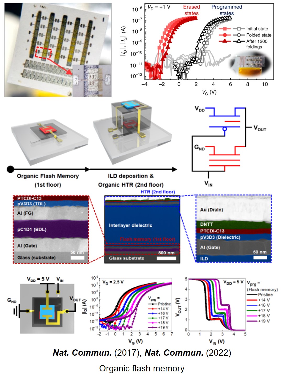
Thanks to the virtue of iCVD-based polymeric insulating layers with a near-ideal insulating property limited by carrier tunneling, an organic flash memory can be designed, in a systematic fashion, based on a tunneling dielectric layer (TDL) / floating gate (FG) / blocking dielectric layer (BDL) structure. The versatile synthetic capability of the iCVD process makes it possible to choose, from the pool of various iCVD-based polymers, a proper insulator that can meet the conditions that are key to the systematic design (e.g., a TDL with low dielectric constant; a BDL with a higher dielectric constant than a TDL). Furthermore, the advantages of the iCVD process, such as low process temperature, solution-free nature, and highly conformal deposition, help one to realize flash memories on various flexible substrates such as PET, ultrathin MylarTM, and paper, which would otherwise be highly challenging to build memory devices on.
|
 |
|
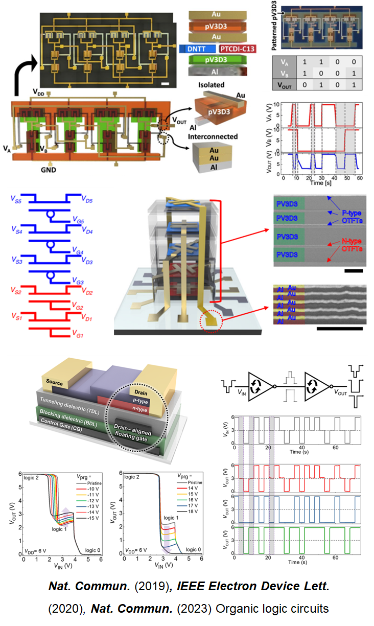 |
Metal interconnection is indispensable for large-scale integrated circuits (ICs) but conventional process cannot be directly adopted for organic circuits due to the high susceptibility of the organic semiconductors against heat and solvent-based developers. iCVD enables in situ patterning of the dielectric layer simply through shadow mask during the deposition process and allows etching-free, via-hole-less metal interconnection. Using this solvent-free metal interconnection, we developed various types of organic logic circuits including CMOS inverter, 6-stage inverter chain, NAND/NOR and even XOR circuit based on four 2-input NAND gates.
Furthermore, we achieved three-dimensional (3D) integration of OTFT circuits using the novel metal interconnect scheme. The highest stacked organic transistors to date, a 3D organic integrated circuits consisting of 5 transistors and 20 metal layers as well as two vertically-stacked complementary inverter circuits that use transistors on 4 different floors are successfully fabricated in a solvent-free manner. Recently, we implemented vertically stacked, low-voltage organic ternary logic circuits including nonvolatile floating-gate memory transistors.
|
|
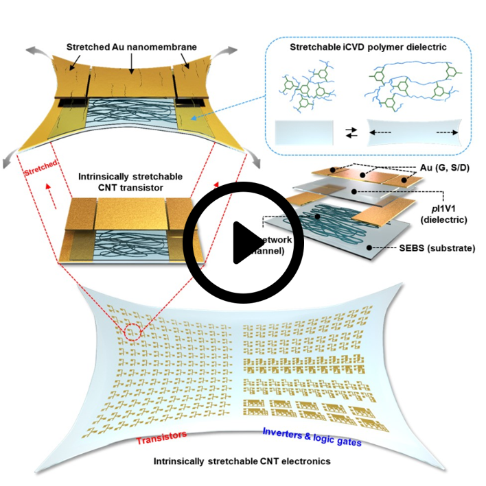
Despite recent advances in materials and fabrication technologies, the development of intrinsically stretchable electronic devices with large-area uniformity, low power consumption and performance comparable with conventional rigid devices remains challenging. A key limitation is the absence of an elastic dielectric material that can be thin and uniform over large areas as well as offer robust insulating properties and high mechanical and chemical stability. We developed stretchable dielectrics that meet these requirements using a vacuum deposition system. Furthermore, we realized the intrinsically stretchable transistor array and logic gates.
| |
 |
|
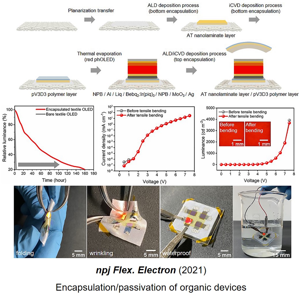 |
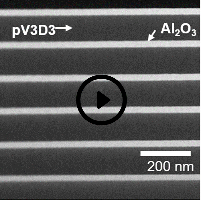
The representative drawback of organic electronics is that most organic materials degrade rapidly upon exposure to water and/or oxygen vapor. Such devices should be encapsulated by a barrier to protect them from water/oxygen vapor under air ambient conditions. Since the solvent-free near-room temperature process allows for the direct deposition of TFE onto organic electronic devices without degrading device performance, iCVD offers many advantageous characteristics for the fabrication of thin film encapsulation (TFE) and has been used to fabricate various types of TFEs by combining the organic layer with inorganic layers obtained through various deposition methods.
|
| Please click on the image to watch the video clip |
|
|
|
|
| Thin film encapsulation |
Stretchable dielectric |
Encapsulation of electronic device |
|
 |
 |
 |
|
|
|