|
|
|
|
|
Functional iCVD polymer films for next-generation electronic devices
|
|
|
|
Thin-film transistors (TFTs) are considered promising candidates for post-CMOS era. They operate as electrically controlled switches and can serve diverse functions depending on the application. A TFT consists of three electrodes (gate, source, and drain), an insulating layer, and a semiconductor channel layer. The insulator critically determines the conductance of the channel by enabling on/off switching. For low-power and reliable operation, electrically stable ultrathin insulators are essential. The initiated chemical vapor deposition (iCVD) process allows the synthesis of polymer thin films that meet these requirements by utilizing monomers with multiple cross-linking sites, yielding robust dielectric layers. As an all-dry deposition method, iCVD avoids limitations of solvent-based processes, such as residual solvents, substrate damage, and poor large-area uniformity, thereby enabling ultrathin, high-purity polymer dielectrics with dielectric performance comparable to inorganic materials.
We developed a library of versatile polymeric insulating layers using iCVD to challenge this common belief and showed that the developed dielectric layers can satisfy a wide range of requirements for next-generation electronic devices. The work on the ultrathin dielectric layers was published in Nature Materials (2015) and led to various further device applications. Currently, the FTFL electronic device team is actively conducting research based on the iCVD process in the following areas: (1) applications to flash memory structures and neuromorphic devices using functional dielectric layers, (2) heterojunction transistor design for multi-stage circuits and hardware computing, (3) stretchable devices, and (4) passivation for electronic devices.
|
|
(1) Flash memory structures for neuromorphic computing
Thanks to the virtue of iCVD-based polymeric insulating layers with a near-ideal insulating property limited by carrier tunneling, an flash memory can be designed, in a systematic fashion, based on a tunneling dielectric layer (TDL) / floating gate (FG) / blocking dielectric layer (BDL) structure. The versatile synthetic capability of the iCVD process makes it possible to choose, from the pool of various iCVD-based polymers, a proper insulator that can meet the conditions that are key to the systematic design (e.g., a TDL with low dielectric constant ~2.2; a BDL with a high dielectric constant ~6.2). In addition, the nearly perfect insulating properties and mechanical stability of the dielectric layer yield excellent retention characteristics and electrical cycle endurance. These features not only support the development of high-performance memory devices but also enable their extension toward artificial synapses for neuromorphic computing. Currently, by employing iCVD dielectric layers containing hydroxyl groups, we have exploited the mechanism in which small voltage pulses induce dipole polarization while larger voltage pulses trigger charge trapping. Based on this principle, we successfully developed a novel device capable of synaptic operation under single-polarity bias. This advancement demonstrates the potential of iCVD-based memory devices to be further extended into neuromorphic systems exhibiting more diverse functionalities.
|
 |
|
 |
(2) Design strategies for heterojunction transistors in AI hardware component
Heterojunction transistors are next-generation devices that utilize p–n junctions as the channel, and depending on the junction configuration, they can be classified into ambipolar transistors, anti-ambipolar transistors, and negative transconductance (NTC) transistors, each exhibiting a distinct form of transfer curve. Their ∪-shaped, ∩-shaped, and N-shaped transfer characteristics enable functionalities that traditionally required complex circuit architectures to be realized at the single-device level, thereby greatly simplifying system design. We design heterojunction transistor structures to exploit these properties. Specifically, we inserted a drain-aligned floating gate into the vertically stacked p–n semiconductor region of an NTC transistor to trap charges, thereby modulating the NTC region. Through this approach, we successfully developed, for the first time, a single transistor capable of reconfigurable binary and ternary inverter operations. Furthermore, in anti-ambipolar transistors, we incorporated separated floating gates beneath the n-type and p-type semiconductors, enabling independent control of the conductance. This configuration allowed for both horizontal and axial modulation of the transfer curve, which enabling Gaussian parameter control. This enables the implementation of a Gaussian mixture model at the device level.
|
|
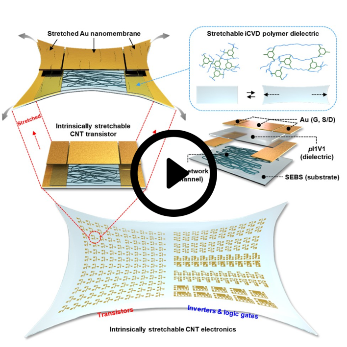
(3) Stretchable electronic devices based on intrinsically stretchable dielectric layer
Despite recent progress in materials and fabrication techniques, achieving intrinsically stretchable electronic devices that combine large-area uniformity, low power consumption, and performance comparable to conventional rigid devices remains a significant challenge. One of the main limitations is the lack of elastic dielectric materials that can be deposited as thin, uniform films over large areas while maintaining strong insulating properties along with high mechanical and chemical stability. To address this issue, we developed stretchable dielectric materials using a vacuum deposition process that satisfy these requirements. Furthermore, we successfully demonstrated intrinsically stretchable transistor arrays, logic gates, and even active-matrix arrays.
| |
 |
|
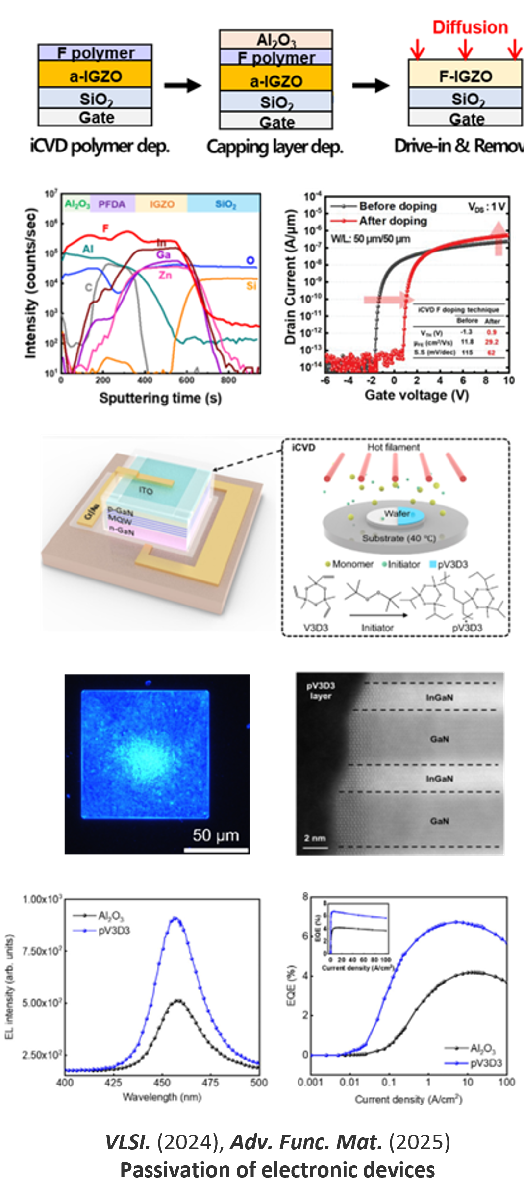 |
(4) passivation of electronic devices toward 3D semiconductor packaging applications
While the development of next-generation electronic devices with novel electrical and mechanical properties is great importance, it is equally critical to elevate the performance and stability of conventional thin-film-based electronics to the level of Si-based technology. The iCVD process not only enables the deposition of dielectric layers for electronic devices but also allows the formation of polymer thin films containing diverse functional groups. By incorporating specific elements into these films, iCVD can provide doping-like effects in semiconductors or enhance device stability through mechanically and chemically robust polymer layers.
First, by employing fluorine-rich polymers, we significantly improved the performance of IGZO thin-film transistors (TFTs), which are widely used in display backplanes and are promising candidates for next-generation DRAM. Since oxygen vacancies (Vo) in IGZO act as shallow donors that supply free electrons, device characteristics are strongly influenced by the Vo concentration. An increased Vo concentration enhances carrier mobility but simultaneously lowers the threshold voltage (Vth), leading to a trade-off. (TFT becomes normally on even at zero gate bias) Fluorine passivation mitigates this trade-off: fluorine ions release free electrons while reducing the Vo concentration, thereby stabilizing Vth near 0 V without sacrificing carrier density. Unlike plasma or ion implantation, the iCVD-based method achieves effective fluorine passivation of IGZO with minimal channel damage and low thermal budget.
In addition, we utilized poly(1,3,5-trimethyl-1,3,5-trivinyl cyclotrisiloxane) (pV3D3) thin films to passivate sidewall defects in micro-LEDs, which are widely applied in display technologies. Since this passivation is achieved under low-temperature, plasma- and solvent-free conditions, it yielded 177% higher electroluminescence and 61% higher external quantum efficiency (EQE) compared to conventional Al₂O₃-based methods. On the basis of these results, our ultimate goal is to realize 3D semiconductor packaging applications.
|
| Please click on the image to watch the video clip |
|
|
|
|
| Thin film encapsulation |
Stretchable dielectric |
Encapsulation of electronic device |
|
 |
 |
 |
|
|
|
|
|
|